
. Credit: IMEC")
3D system-on-chip (3D SOC), enabled by electronic design automation (EDA) and 3D process technologies, is an attractive heterogeneous integration approach for addressing the memory wall in high-performance systems.
Further performance gains at the system level can be achieved when the backside of one of the integrated wafers is exploited for either power delivery, signal routing or both.
In this article, Dragomir Milojevic, Geert Van der Plas and Eric Beyne shed light on these promising approaches.
The benefits of 3D-SOC design and of backside interconnects in specific circuits are highlighted in two papers presented at the 2021 IEEE International Electron Devices Meeting (IEDM).
Promises of a 3D-SOC design approach
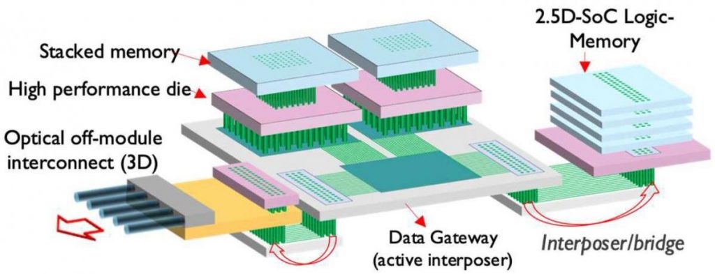
Data-intensive high-performance systems intended for advanced computation, data server or deep-learning applications increasingly suffer from the so-called memory wall—the challenge of accessing data quickly enough. An interesting approach to tear down this memory wall is 3D system-on-chip (3D SOC) integration. Following this heterogeneous integration approach, the system is automatically partitioned into separate chips that are concurrently designed and interconnected in the third dimension.
In their invited 2021 IEDM paper ‘3D-SOC integration, beyond 2.5D chiplets,” the authors explain how this 3D-SOC concept goes beyond today’s popular chiplet approaches for realizing multi-chip heterogeneous system integration. Eric Beyne, senior fellow, VP R&D and program director 3D system integration at imec: “Chiplets involve separately designed and processed chiplet dies. A well-known example are high-bandwidth memories (HBMs)—stacks of dynamic random access memory (DRAM) chips. This memory stack connects to a processor chip through interface buses, which limit their use to latency-tolerant applications. As such, the chiplet concept will never allow for fast access between logic and fast, first and intermediate level cache memories.”

With 3D-SOC integration, memory-logic partitions can be realized using direct and shorter interconnects—resulting in significant performance improvements. In their invited paper, the authors show an optimized implementation of a 3D-SOC design with memory macros in the top die and remaining logic in the bottom die—resulting in a 40 percent higher operating frequency compared to a 2D design.
They also discuss the key challenges of realizing fully functional 3D SOCs. Dragomir Milojevic, principal scientist at imec and professor at Université libre de Bruxelles: “On the design side, a 3D-SOC co-design strategy is needed for both logic and memory partitions. This requires dedicated electronic design automation (EDA) tools that can handle both designs simultaneously, using automated tools for system partitioning and 3D critical path optimization during place-and-route. Through our collaboration with Cadence, we have access to these highly advanced tools.” On the technology side, progress in wafer-to-wafer hybrid bonding solutions will allow for very high chip-to-chip interconnect densities, mandatory for partitioning of first and intermediate level cache memories.
The next step: exploiting the wafer’s backside
A possible partitioning of high-performance 3D-SOC systems involves some or all memory macros to be placed in the top die, while the logic is placed in the bottom die. On the technology side, this can be realized by bonding the active frontside of the ‘logic wafer’ to the active frontside of the ‘memory wafer’ by using a low-temperature wafer-to-wafer bonding technique. In this configuration, the original backsides of both wafers now reside on the outside of the 3D-SOC system.
Eric Beyne: “We can now think of exploiting the ‘free’ backside of these wafers for signal routing or for directly powering the transistors in the ‘logic wafer.’ Traditionally, signal routing and power delivery happens in the wafer’s frontside, where they compete for space in a complex scheme of back-end-of-line interconnects. In these designs, the wafer’s backside only serves as a carrier. In 2019, simulations by Arm for the first time showed the beneficial impact of using a backside power delivery network (BSPDN) in the design of a central processing unit (CPU), that implemented a 3nm process as developed by imec. In this design, the interconnect metals residing in the wafer’s thinned backside connected to 3nm transistors in the wafer’s frontside using through-silicon vias (TSVs) landing on buried power rails. Simulations revealed that this BSPDN was seven times more efficient than the traditional frontside PDN.”

Additional performance gains can therefore be expected when BSPDNs are implemented to supply the power-hungry core logic circuits that reside in the bottom of a ‘memory-on-logic’ 3D-SOC. One could also think of alternative 3D-SOC partitions where part of the memory tiles (e.g. the L1-level caches static random access memory (SRAM)) reside in the bottom die as well, also powered from the backside.
Besides extending the possibilities for 3D-SOC designs, BSPDNs have also been proposed for monolithic single-chip logic and SRAM systems-on-chip (SOC), where they can assist further device and IC scaling. Geert Van der Plas, program manager at imec: “Moving the power delivery network to the chip’s backside has proven an interesting approach to address the back-end-of-line (BEOL) routing congestion challenge and reduce the IR-drop. A main difference with the 3D-SOC approach is that a dummy wafer is now bonded to the target wafer to allow for backside wafer thinning and metallization.” One of imec’s partners recently announced to implement such a BSPDN concept in one of its future node chips.
Backside interconnects to further improve performance of SRAM macro and logic
While the benefits of a BSPDN could already be demonstrated in specific designs, additional gains can be expected from using the wafer’s backside for global signal routing. Imec, in collaboration with Cadence, has for the first time assessed and optimized SRAM macro and logic circuit designs that are partly routed from the backside. An SRAM macro not only involves the memory bit cell arrays but also the peripheral circuitry (like address decoders, control block etc.)—relevant for processor design.
For both SRAM macro and logic, up to three backside metal layers were used for signal routing, while nano-TSVs (nTSVs) connect the backside metallization to the frontside. The SRAM macros implemented 2nm nanosheet transistors in their design. In these macros, only the global routings for the peripheral circuit were designed with backside metallization. For logic, a ring oscillator framework was used to assess the impact of backside signal routing. The design implemented forksheets of the 2nm technology node in the logic standard cells. A physical implementation of a 64-bit ARMTM CPU using the same 2nm forksheet process design kit (PDK) is used to ensure the meaningfulness of the ring oscillator simulation results.

Geert Van der Plas: “Compared to frontside routing, backside routing turned out significantly more beneficial in improving delay and power efficiency for long interconnect signal routing. For the SRAM macros, we demonstrated up to 44 percent performance improvement and up to 30 percent power efficiency improvement compared to frontside routing. For logic cells, backside routing enabled 2.5x speed improvement and 60 percent energy efficiency increase.” The results are described in the 2021 IEDM paper “Design and optimization of SRAM macro and logic using backside interconnects at 2nm node” by R. Chen et al.
Assessment of the circuits’ performance and power efficiency was enabled through a combination of experiments and modeling. Dragomir Milojevic: “Experiments involved an optimization of nTSV processing in terms of capacitance and resistance—to ensure a good electrical connection between the frontside and the backside metals. These parameters were fed into a model, used to perform the simulations. Finally, our team performed a design-technology co-optimization (DTCO)-driven routing optimization which showed a path for further improvements. We demonstrated an additional 20 percent performance improvement by reducing the capacitance of the backside metals.”